Technology

Principle
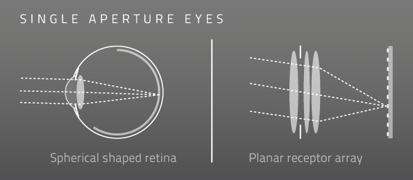
Conventional cameras have their natural antetype in the eyes of mammals providing "eagle eye" high resolution at the cost of rather bulky and therefore heavy optics. The single aperture objectives consist of several lenses required for generating an image of high fidelity. If extreme miniaturization and lightweight construction is required, Mother Nature goes for multi-aperture objectives known as facet eyes found in insects and spiders. These eyes consist of several adjacent imaging channels formed by individual micro-lenses and photo receptors responsible for imaging a part of the entire object field. facetvision's imaging systems are inspired by the multi-aperture compound eyes translated into artificial, technical systems based on CMOS and CCD imagers and microoptical lens arrays providing high resolution, extreme miniaturization and cost-effective production.
Ultra-Thin Microscope
Microscopes are imaging systems used to visualize small objects and structures which cannot be seen by the naked human eye. The appearance of the instrumentation was not least defined by the work of the Jena pioneers of microscopy: a cylindrical tube of about 150 mm length with an objective at one end facing the object and an ocular at the distal end which is looked through by the examiner's eye. The newly-developed ultra-thin imaging system possesses a significantly different morphology but still uses principles of the conventional layout and is dedicated to the same goal of a μικρός (small) σκοπεῖν (watch). The advantages of the multi-aperture layout are twofold: first, it allows for a reduction of the total track length to 5.3 mm, and second, the simultaneous examination of large object fields of almost arbitrary extent with a lateral resolution of 5 µm. Current systems are based on full format imagers (36 x 24 mm²). The imaging optics is based on adjacent channels each transmitting a part of the entire object. The high spatial resolution is achieved by employing a complex lens stack using aspherical and achromatic micro-lenses. The new optics concept of the ultra-thin microscope enables new applications in the fields of life science imaging, sensors and machine vision.
Ultra-Thin Camera
Conventional cameras based on a single-aperture concept are limited in their miniaturization due to physical constraints. facetvision's multi-aperture imaging optics concept enables thinner objectives better suited to integration in ultra-slim mobile devices such as smartphones and laptop computers. The key to the miniaturization is twofold:
first, the camera’s entire field of view is split into separate, individual parts imaged by each optical channel which are electronically stitched together in order to create the overall image. Second, a comprehensive and synergetic system design taking advantage of state-of-the-art micro-optics fabrication, novel image layout based on industry-ready CMOS-fabrication and image post-processing by adapted software algorithms. This makes the system viable for applications in the fields of consumer electronics and automotive.


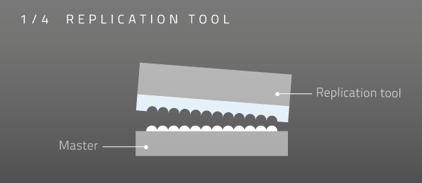
facetvision's optical fabrication technologies rely on parallelized processes for the generation of micro-optical components which differ from conventional lens fabrication by grinding, polishing or injection molding, as the goal is to merge optics and electronics in design, function and fabrication. As in the semiconductor industry, wafers instead of single pieces are handled for process parallelization, enabling high reliability, miniaturization and low cost production. Equipment, processes and materials as found in the high-precision semiconductor industry are used and adapted, based mainly on lithographical techniques, leading to optical devices produced by optical machines. The low-cost and high-precision micro-lens fabrication uses an imprint process of an ultra-precise stamp replicated into a liquid material which hardens when illuminated by UV light. facetvision controls the entire process chain from optical design (ray tracing), to mastering (diamond turning, milling and shaping; laser lithography), replication (UV replication on 8"), stacking, bonding (UV cure) and final dicing (cutting blade, laser ablation). In some cases, ASIC imagers are required in order to achieve optimum performance, ensuring the synergetic layout of optics, electronics and software. While the design is done inside facetvision, the production takes advantage of semiconductor fab services.

 Fraunhofer Institute for Applied Optics and Precision Engineering IOF